Overview: After the invention of Transistors in 1947-48, the trend towards “miniaturization of integrated circuit” (the technology of putting many no of ICs into single silicon chip) opened the door of modern electronics on the wider scope in a lesser space. If we go the whole hog, we find that the journey chip design technology right from SSI (12 gates) to VLSI (>10000 gates) is remarkable and its rate of growth is unbelievable & and some times becomes unpredictable. Let us have overlook on the development in IC technology from the start of modern era of electronics (1948) to present in statistical facts and figures.
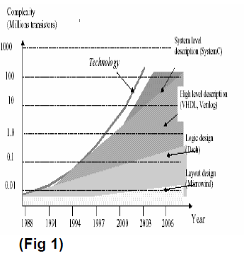
A. IC Design Technique from layout level to system level
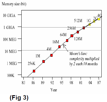
C. Evolution of Memory Size
Evolution of Memory Size The First 1 kb memory was produced by Intel in 1971. Later on Semiconductor memories have advanced both in density as well as performances. With the production of 256 Mb memories in 2000 and 1 GB in 2004, it has revolutionized the computer and telecommunication industry. According to the estimates, it is expected to increase up to 16 GB in 2008.
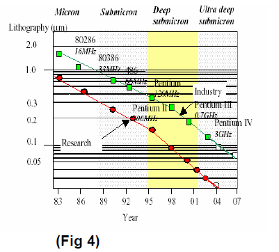
D. Evolution of Lithography
Trend towards the smaller dimension has been accelerated since 1996.In 2007, the Lithography is expected to decrease down to 0.07 um. Fig 4 depicted below gives the picture of lithographic revolution.
E. Technology Generation Forecast:
Moore’s law says that Minimum transfer of feature size must decrease by factor of 0.7 every year but trends are more than that. It can be clear by the graphical data given below in fig 5.
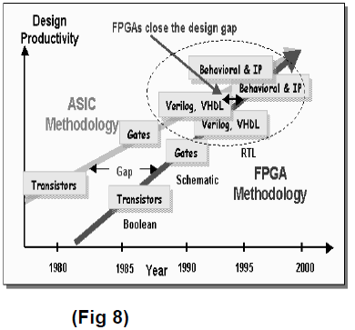
Programmable Logic Devices is that interconnects of CLBs are also programmable and it has in built Block RAMs which are not available with CPLD. All the basic differences between ASIC and FPGA has been depicted below (Fig8) and can be easily understood.
F.1.1 ASIC VS FPGA
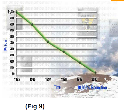
F.1.2 New FPGA Price Revolution:
Price wise also programmable ASICs are more advantageous. The considerable decrease in their prices has opened space for even smaller companies and design houses to work with technologies for their medium to high level products whose gate counts is up to around 5 million gates. The new Vertex 5 FPGA by Xilinx has this capacity and it is expected to increase by 10 million gates in the near future.
It is given below:
General Design Productivity
= output produced /labor expended
= output per unit worker hour
Manufacturing productivity = value added/labor expended
= value added per unit worker hour.
= (end product selling price- material cost of the Product) worker hour
= dollars per worker hour
Chip design productivity ? Transistor /gate per unit engineering effort.
Chip design productivity
= chip design complexity/ engineering effort.
= complexity per unit engineering hour.
= normalized transistors per person-hour.
Because of the complexities in Chip design productivity as it is defined as chip design complexity per unit engineering hour not as transistors /gate per unit engineering hour (as in the general case), It takes much time to come to market and also it requires sound knowledge of all manufacturing cycles, otherwise it may cause huge cost to the production loss.
H. Latest Chip Design Trend:
The trend for whole systems design, now a days is embedded i.e the use of hardware and software for the specific applications because of the disadvantages of only hardware or software solution. In that because of the programmable and re configurable, re –usable nature of FPGA, the widespread use of FPGA has been become real trend. FPGA are widely used in Networking (PCI, Ethernet, USB), DSP & Communication, Speech Processing & Image processing, Tele mobile communication, Micro processor & Micro controller Based System., Home appliances etc. sectors which has played significant role in 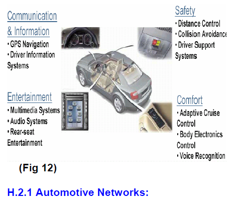
H.2.1 Automotive Networks:
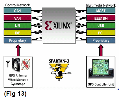
The Car multimedia system basically uses to interface with Xilinx FPGA which consists of CAN, VAN, LAN, MOST, IEEE1394, and USB & PCI etc given below (Fig 13).
H.2.2 other issues and challenges before automotive sector
a. Integrating different standards Networking: MOST, CAN Video: LVDS
System Interface: PCI
b. System control and peripherals
c. Micro controller and microprocessor obsolescence
d. Offloading hardware intensive blocks from host CPU
e. Software defined Radios
f. High performance memory support(DDR/SDR)
g. Interfacing to Various Flash types(CF+,MMC/SD)
h. EMI Signal Management
i. Display Control
Basically the medical expert system (MES), given in Fig 14, is composed of FPGA, the RAM for intermediate store of artificial neural networks output, and the memory that contains the weights. The input MUX is used to select inputs for the FPGA module either from previous results or from the user and the configurations RAM that holds the configuration bit stream for the FPGA. The weight and configuration RAM’s are loaded externally which allows the easy update of the system.
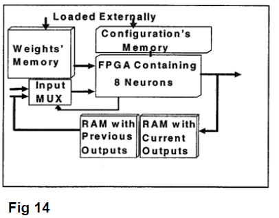
This system is very much of use in the detection of pulmonary diseases like Physical exams, cough, fever, chest pain, haemoptysis, dyspenia, wheezing, sputum, and other historical data etc.
H.6 Bio Chips: A Medical Revolution
The development of Bio chips to sequence unknown genes and to study gene expression is great idea. But the working principle suggests that they can be used for engineering applications that require parallel processing. DNA chips are proposed here as the physical substrate to store and evaluate a set of rules for knowledge based systems.
H.6.3: DNA Scanner for Human Diseases
Now efforts are being made to use DNA chips to test dreaded disease into human body. Few companies of USA and South Korea including Vidar Systems.Inc (www.vidar.com) and StarVRay co.,Ltd (www.starvray.com) have recently developed DNA scanner which will be very much of use in detecting dreaded diseases like Cancer, AIDS, TBs etc. As per design, chip will be fitted inside the DNA scanner module, which will exam DNA test of the individual and it will compare with all the test properties inside chip. Then automatically disease will be pointed out by this DNA scanner and can be shown on PC screen too. One of the good things in this product is that you can put at most 4 chips at a time.
H.7 Neuro Chips
Recently revolutionary Invention of Neuro Chip wondered the world: The beauty of this neuro chip is, if it is inserted into our nervous system, it will control Brain’s nervous system and then according to the program one can control on his thinking ability too. This is the excellent product, will be used for many medical and other purposes. Can we say that designing dreams are also not impossible? H.8 Control systems for Robotics Applications Now a day, Robotics application has gained momentum in a very wide area of scope. Technically this requires applications of convergence of many technologies to perform multiple tasks at the same time. General controller has very little scope where as FPGA chips as controller has much more to play which can be re- used, and re-configured by multiple numbers of times. The reconfigurable architectural properties of FPGA has opened the door for much more things to be added for the controlling applications
J.concluding Remarks:
As technology grows,many more problems usually come for the solution which helps industry to row and finally customers get benefited as result of the practical implementation of those technologies and solution of those problems. In the field of chip design and development, the rates of advancements are unpredictably fast. Its very tough to conclude here because many unknown facts which I missed here, many kno examples of recent trends which I could not mention, many technological changes which have already taken place in the fast changing world of Chip design which I don’t aware of . I can not conclude as it is an unfinished journey! |
|
The introductions of HDLs have made possible the design of complete System on Chip (SOC), with the complexities rising from 1 million to 10 million transistors. Recently System C has been introduced for 100 million to 1000 millions of transistors
B. IC Design Growth at frequency level
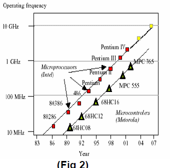
The clock frequency increased for high performance micro processor and industrial micro controllers with the technology scale down. Here Motorola micro controller has been taken as the example used for high performance automotive industry applications.

F. Evolution of Programmable Devices and its trend
F.1 FPGA Architecture:
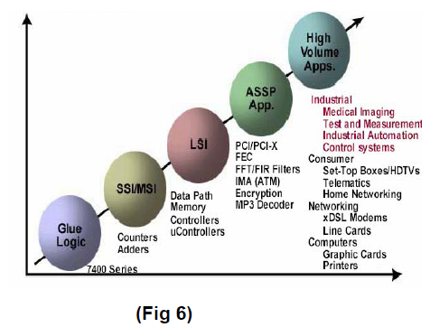
The fig 6 depicts and describes the fast journey of miniaturization of integrated circuit from Glue logic to High volume ASICs along with its large volume of application. As per trend, the use of Programmable ASICs i.e FPGAs are growing by leaps and bounds at least for their implementation into medium to higher end design products which give the best possible solution in terms of less time to market, portability, less design complexities and reliable quality.
Xilinx is one of the best companies in the world for producing programmable ASICs. Its percentage share in the production of FPGA is highest.
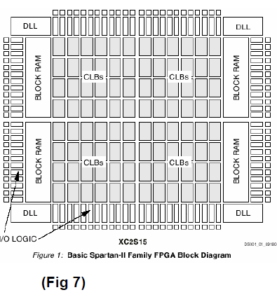
The basic element of the FPGA is Configurable Logic Block which consists of programmable gates, flip flops and muxes etc along with BLOCK RAMs. The major advancement of FPGA over CPLD, Complex
F.1.3 Cost Management through System Integration.
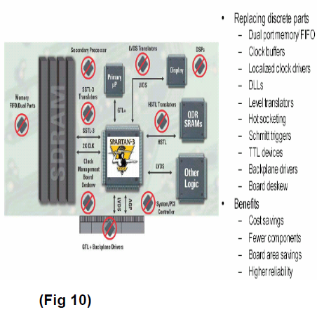
The sharp decline in the prices of FPGA with its improved facility, better performance, and greater density of gates made the task of system integration easy. Because of this even large systems can also be designed and implemented into FPGA chip that gives cost effective and reliable solution to the customers. Fig 10 describes how Spartan 3 FPGA integrates with many other ICs and hardware components.
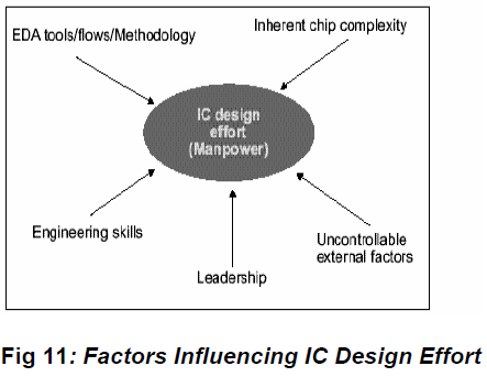
G. Chip Design Productivity and complexity:
As chip size is shrinking, the logic of its design and technology of their production going to be more complex. The factors of the total engineering effort (fig 11) affect the chip design productivity and also the manufacturing productivity which is much more complex and unpredictable.
revolutionizing chip design and manufacturing industry. In addition to these mentioned application areas, some of the areas given below which have been given most attention by corporate world as these are few of the latest trends in Chip Design Industries.
H.1 Real Time Audio and Video Processing:
The reconfigurable FPGA systems design and re-use of FPGA chip is basically good example for real time image processing systems. The real time image stabilization problem caused due to jittering images will be solved by the use of this reconfigurable system design.
The use of high powered handy cam, Webcam and the use of efficient jittering algorithm in it are more appropriate example. High quality handy cams are now jitter free images which occur due to hand shakes or the internal shift in the image axis.
The use of FPGA system in Noise cancellation and Noise reduction has also gained momentum. This has been already implemented in Railway station in Korea, Japan etc countries. Now efforts are being made to implement it on Airports. The scientists are working in the direction of 100% cancellation of noise which is practically looks impossible but if it is implemented it will have capacity to revolutionize this industry in many ways. Samsung Electronics, IT Magic (
www.itmagic.co.kr ) and other companies in Korea, Japan and USA are working on for complete cancellation of Noise.
H.2 Auto motive Sector
The FPGA solution for the car with all multimedia system is the latest trend in the market in the automotive sector. The use of GPS system as tool for communication, information’s, safety and collision avoidance mechanism along with all accessories of entertainment with great extent of comfort has gained momentum in the developed to developing countries. It is the need of time also when your kid has to come back to home from school without help of any driver or parents. Mean to say, high powered robot will do all the works. Scientists are working to make robotic systems inside the car for this purpose. Presently In the market, car multimedia system has been implemented but this is without robotic system. Let us hope, it will come very soon. j. Content protection/encryption
k. Industrial temp parts
l. Overall cost management
m. Dynamic nature of products
H.3 Biometric analysis for Security
The implementation of Biometrics security systems by using best encryption and decryption algorithms into VLSI FPGA technology is a challenge for the scientists. This is the best possible solution for the security particularly in defense, military, aerospace centers and other important govt and private offices where identification of incoming and outgoing people are required.
H.4 System on chip with virtual component:
In the recycling age, designing for reuse sounds like a great idea but with increasing requirements and chip sizes, it is not an easy task. System on Chip may contain both a system bus connect and Peripheral bus connect custom I/O block that provide functions not commercially available, may also be included.
H.4.1 Adv. of System on Chip
1. Increased levels of design reuse.
2. More effective hardware-software
Co-design. 3. Better trade-offs between general
Purpose vs. domain-specific architectures and algorithms. 4. Greater integration of functionality
on-chip (hardware-software, analog- digital). H.5 Neural network & Artificial intelligence for Medical Expert system:
Recently using Artificial Neural Networks (ANN), Medical Expert System (MES) has been introduced which will be used for diagnosis of pulmonary diseases. This is based on the cascade of three layers of artificial neural networks that process disease symptoms and other inputs data, and provide as outputs the possible pulmonary diseases with accuracy 90%. The third layer of structure, which has not yet been designed and implemented, may suggest possible medical treatments and medicines, according to the result of the previous layers.
H.5.1 Overall MES Design
H.6.1 Bio Chips: Design Steps
Following are the steps involved in designing Bio chips
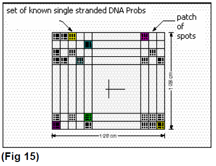
1. In DNA chips, each cell uses millions of copies of DNA sequence called probes. The colors indicate that probes are different between cells
2. DNA sequence tagged with the quantum dots. Small dot is the quantum dot.
3. Complementary probes and target bind to fluorescent DNA helix. In practice, there are millions of probes per cells, so millions of targets are required to produce Fluorescent cell after hybridization
4. Plant states are sampled and A/DNA Converter produces millions of two tagged DNA sequences. Small dot is quantum dot used to identify helix
5. DNA chip is injected with millions of tagged DNA strands. After scanning the chip and processing the rules o/p is produced
6. DNA chip can be used to detect faults in the plant. State variables are sampled, converted into DNA target and injected into chip. The green cells are fluorescent probes after being excited with UV light
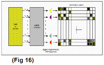
H.6.2 Look up tables as DNA Chips: Rule Based System for Plant Analysis
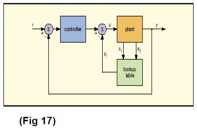
Basically, look up table is derived from the past experience and it can be used to improve the performance of the closed loop with an existing controller (fig 17).
The rules are stored on the chip and the evaluation of the complete rule base at each sampling instant is carried out in parallel using the hybridization of DNA strands speed, high density, low cost and low power solution.
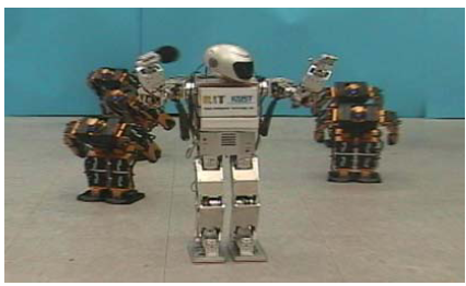
H.8.1 Glimpse of Dancing Robot:
Recently a small_sized humanoid robot, SaRam, Fig 18, made by Robot Intelligence Technology (RIT) Lab of Professor Kim, Jong-Hwan in Korea Advanced Institute of Science and Technology (KAIST) has made great contribution in the field of robotics in association with six Robonovas, made by Mini ROBOT Corp. They formed a heterogeneous robot team, RoboBees; which exhibited "robot dance", a new genre of robotics technology. Mr. Naveen Kuppuswamy, a MS Student from India in RIT Lab who was deeply involved with this project admits that, FPGA Technology has major role to play in the improvement in his Dancing Robot and for all other robotics applications.
Challenges before chip Design industry
Insted of many revolutionary design outputs given above, many issues which are left, has to be paid more attention and it have become challenge for the designers. These issues require close interaction and collaboration for trade-off and optimization by all design, device, and process fields. These are
• Design/device/process optimization and trade-off for leakage current, power consumption, & noise issues in mixed-signals, large scale IC devices, or design re-use. •Incorporation of new materials (i.e.dual gate, multi-material active layers, etc.) in IC cell library and design of advanced transistor structures (i.e. Double Gate FDSOL,FinFET,ftc). About The Author: The author is Technical Chip rchitect working in the field of medical imaging and DNA scanner based chip design and development with Korean chip design company “StarVRay Co., Ltd (www.starvray.com) at Daejeon city of South Korea. The author is also the chairman of BiharBrains (www.biharbrains.org) and chief editor of Manthan. Note: This article is based on the other lecture IEEE,PTC,chapter,pune India in dec 2003 on in the topic “Chip design Trends and Fabrication Prospects in India”. This article with few updates and modification has been divided into two parts, i.e (1) Emerging Chip design Trends and (2) Fabrication prospects In India. The Detailed information about Fabrication Prospects in India will be published in the next issue of the Manthan on the titled “Indian Chip design Industry”. |