|
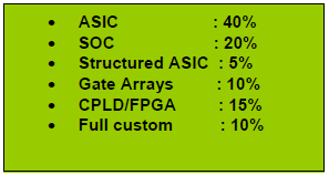
Though in India ,manufacturing chip is still dream but certainly as far as chip design activity is concern, Indian chip designers has been regarded as expert and going to be leader in R& D activity. Till today, the bulk of the chip design activity in India is mainly focused on ASICs and FPGAs, processor based SOCs are proliferating now. The estimates says that the types of IC design is being done in India in today is based on following
From the end product prospective, most chip design in India is targeted at 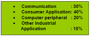
Approximately 50 percent of the design activities in India are carried out in the areas of wireless and wired communications. Consumer electronics represents the next-largest application. Designs at geometries of 90 nanometers and larger comprise approximately 90 percent of the total design activities in India.
While captive design centers increasingly are engaged in high-end R&D projects intended to
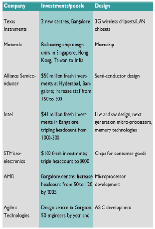
Three years ago, TI India opened centers for designing 3 G wireless chipsets and LAN Chipsets. From being an outpost experiment 20 years ago, Texas Instruments today drives research at TI, outside the US.
2. Intel Corporation: Intel, the world’s largest microprocessor player, with a stranglehold in the PC, notebook and server market began its tryst with India in 1998. It started out with a pool of 3000 engineers but is now in the process of increasing its headcount three-fold within the next three years. Engineers at Intel’s centre in Bangalore started out by being involved in system engineering and software design. Now they’ve moved up the value chain and are responsible for development of next generation microprocessors, semiconductors and memory technologies.
3. Cadence Design Systems: Cadence, which is a world leader in design automation, is putting $50 million into its Indian operations.
Famous Chip maker Advanced Micro Devices established a chip design center in Bangalore, India, for use in next-generation designs. It has plans to invest approximately $5 million over the next three years to establish the center and ramp up operations, which will initially employ 40 engineers but could be expanded to as many as 120 by the end of 2005. The center will be known as the AMD India Engineering Centre Private Limited.
5. Motorola: Motorola is relocating its design house from Singapore. Hongkong, Taiwan to India .Micro chip is its product widely used in the market. 6. Mentor Graphics: The automation firm, Mentor Graphics, plans to double its engineer man-count in three years.
7. ST Microelectronics: The world’s third-biggest microchip manufacturer recently added a new wing with a built-up area of 70,000 square feet at its advanced chip design centre in Noida, on the outskirts of Delhi, to accommodate 550 additional software engineers who work on chip design, embedded software and also provide software service backup for STM’s global clients. The designs that are finalized go into proto-typing chips, which are mass produced in fabrication centers like Singapore and Taiwan
If you go whole hog of the business of the Indian chip industry, we may summarize that Indian chip industries are mainly in the field of design & services or work at the subsidiaries of the global chip companies particularly in the field of hardware services and board manufacturing, system integrators, software IP firms. Industry leaders believe India is becoming a 'VLSI design store' with a strong presence in Intellectual Property development, integration and embedded software services.
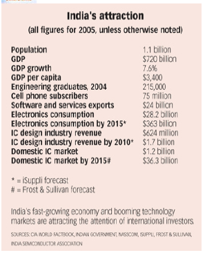
The total design revenues of the sector stands at $3.5 billion in 2005 and is expected to grow almost 15 times by 2015.
According to a market research firm, in 2003 the total electronics market in India was estimated to be $12.3 billion. The market is attracting very serious attention—both from domestic and international players. It is estimated to touch revenues of $800 million for ASIC services while embedded software expected to reach $1500 million.
According to government and industry estimates, India's electronics hardware market could grow from $28 billion in 2005 to $363 billion by 2015.
The government is expected to take an equity stake in a $3 billion Hyderabad chip factory with start-up SemIndia, which has a partnership with AMD.
Fab lab does not exist in India: why?
1. Huge Fabrication lab cost:
The actual problem is that quality talent with the right skills is becoming scarce. The skills required are in vertical domains (DSP, telecom etc.) along with in-depth understanding of chip design challenges like designing for high speed, low power, small size, handling large complexities, accounting for deep sub-micron effects like signal integrity. This is assuming that these engineers come with basic microelectronics skills including an understanding of semiconductors and design basics like language-based design methodologies. Exposure to contemporary design tools is also important.
2. Design Incompetence, Probably India is not prepared
According to Mr Girish of Texas Instruments, "It's not feasible for many small Indian companies to make sustained investments for a long period of time, which is required for product development (including the area of chips design/manufacture). I don't think we can do that now. Also, to get into full-scale manufacturing, the government should also take some efforts. It has to take a decision to shift manufacturing units to smaller towns instead of concentrating on the metros.“
ISA: The latest is the ISA, or Indian Semiconductor Association, whose aim is to promote India as a destination for commercial chip fabs and develop “clusters” of fabs that the world can come and use. The chip fabs, says Poornima Shenoy, president of the year-old outfit based in Bangalore, will “encourage local manufacturers to become important worldwide players in electronics.” The association has 104 members, but they are all chip design houses including heavy hitter Broadcom. The group is hoping that manufacturing will happen and those new players will participate.
Efforts to bring Fab labs in India
Nasscom: Just about everyone has heard of Nasscom, the powerful Indian software industry association. Now other groups are popping up along India’s technology corridor to try and mimic
ISA’s dream is to develop a physical fab city like Hsinchu Park in Taiwan. It has scope for employment too, because Hsinchu Park, Shenoy says, has 250 ancillary units which require physical labor, and about 200 design houses as well. “These are what seed electronics products,” says Shenoy, adding that the whole eco-system, if it comes together, will create 3.6 million jobs by 2015 in India, and “will be one of the biggest drivers of the economy.”
Allied Material, a US based equipment manufacturer and a group of Indian equipment manufacturing companies are contemplating a chip manufacturing plant in India. Despite being considered an IT superpower, India still waits for a fabrication facility for semiconductor wafer. India has design, assembling and testing capabilities, and global leaders like Nokia, Motorola and Ericsson are all set to open production plants in India. The only missing link is a chip fabrication unit.
Govt Incentives: Government support for India’s technology industry has strengthened dramatically since the 2004 election of Prime Minister Manmohan Singh, an Oxford-trained economist and former central banker who has welcomed foreign investment and helped liberalize the economy. Recently, the government identified the semiconductor industry as a particularly high priority. Finance minister P. Chidambaram declared during his annual budget speech to parliament in February that “the time is ripe to make India a preferred destination for the manufacture of semiconductors.” His 2006 budget calls for a three-year program to encourage chip makers to set up factories in India. A detailed national semiconductor policy is still being drafted, but the incentives for qualifying projects are expected to include tax breaks, loans and the option of equity investments through India Infrastructure Finance Co.
India will need to spend heavily to compete with other countries’ incentives. China, Ireland, Israel and Malaysia, for instance, reportedly offer much higher tax breaks to semiconductor makers $540 million grant to persuade Intel to build a $3.5 billion fab there.Union Minister for Communication and Information Technology, Dayanidhi Maran, has taken up the challenge to bring as such a facility to India. The ministry has given six months time to the interested companies to come up with a proposal. The plant would need an investment of about $3-4 billion. The centre government has to put any money into the older fabs,” he insists. Government officials aren’t tipping their hand yet, but a recent Indian press report quoted an unnamed senior government official as saying that prospective fab developers will have to invest at least $1 billion in India to qualify for government loans and equity investments. If true, that could hurt some of the smaller projects’ chances.
Three of the five groups are planning 8-inch fabs, at least for their initial stages. Nano-Tech Silicon India broke ground outside Hyderabad in June 2005 on what was to be a $600 million 8-inch fab. But recent visitors to the site say that no construction appears to be under way. And despite sporadic Indian press reports about possible tie-ups between Nano-Tech and IBM (and more recently Intel), there have been no recent statements from the project’s organizer, Korean businessman Pyung June Min, to clarify whether his company’s technology and investment partners are still in place.
Another 8-inch fab was proposed last year by India’s Nest Group, a diversified electronics conglomerate that announced plans to build a $1 billion memory foundry in India’s Kerala state, with backing from Japanese partners. The company has said little about the project since then, however, and did not reply to inquiries from ELECTRONIC BUSINESS. Company officials have said they plan to open a chip design center this year and a chip test and assembly plant in 2007.
HSMC plans to start by relocating an existing 8-inch production line to India. The company’s $500 million first phase calls for taking over a 180- to 130-micron manufacturing process, and all the necessary fab equipment, from an as-yet-unnamed U.S. chip maker seeking to outsource some of its production. Verma says his group will continue producing chips for the seller after moving the operation to India. It also plans to use the 8-inch fab for technology development and engineer training while building a second, $3 billion 12-inch fab.
Even SemIndia, which aims to ultimately build a $3 billion 12-inch fab, plans to get its feet wet in India first with a chip assembly and test operation. Agarwal calls the assembly and test facility,
|
|
serve the needs of the global parent company, the role of IDHs in India is rapidly growing as these companies provide flexible business models for design engagement.
Most of the IDHs in India are involved primarily in front-end design work, providing testing and verification-level services. However, a few of these companies also are involved in end-to-end design activities, ranging from specification to tape outs.
Overview of major players of Indian Chip design industry: As per estimates, more than 100 good companies are working in the ASIC/FPGA design and more than 150 companies are working in embedded chip design and development spread over all over India particularly in the major cities like Bangalore, National Capital Region, NCR (Delhi, NOIDA, and Gurgaon), Pune, Hyderabad, Chennai, Mumbai etc. In addition to this Chip design industry is also gaining momentum in Kolkata, Chandigarh, and Mysore, Vishakhapattnam, Coimbatore and Bhubaneshwar cities of India. The following major companies have played major role in this industry, these are
1. Texas Instruments : When Texas Instruments became the first multinational technology company to set up a design base in India In a period of 20 years Texas Instruments (TI) has erected more than two design centers—over two third of the engineers at these centers are involved in designing integrated chips. But much more important is the fact that virtually every TI design worldwide uses some design proto-typed in India. The centre delivered the world’s first single-chip solution for high-end modems.
before being fitted into a range of electronic goodies ranging from mobile phones, DVD payers, mart cards to personal digital assistants, etc.
Other leading names are IBM Global Services, Lucent Technologies, Philips Semiconductors, Texas Instruments, Motorola India, Cypress Semiconductors, HCL Technologies, ST Microelectronics, GE India, Bi Square Consultants DCM Data Systems, Artech Information Systems, Alliance Semiconductors, Analog Devices, Core El Logic
Business Growth: Present & Future
The market is enormous. The ASIC design services market globally is estimated at $50 billion in 2006, while the embedded software market size is put at $25 billion. The fabless trend continues to soar and the US Fabless Semiconductor Association predicts that the market shares of fables companies will jump from just over 10 percent today to 50 percent by 2010. Additionally, there is the IP design market opportunity. iSupply Prediction: India's Integrated Circuit (IC) design industry is booming, with market revenue expected to reach US$2.1 billion by 2010, rising at a Compound Annual Growth Rate (CAGR) of 29 percent, up from $596 million in 2005, iSuppli is predicting
By 2015, the design market in India will grow to 15 times the size it is today and the market value of the design industry will be 1% of the nation’s gross domestic product (GDP), according to researcher iSuppli.
As these Indian companies continue to mature in terms of experience and capabilities, iSuppli projects that their contribution to the total market will grow to 49 percent by 2010, up from 35 percent in 2005.
Effect of IC Industry when we get fab lab in India
The Semiconductor Industry Association (SIA) reported that global semiconductor sales set a new monthly record for the fourth consecutive month. Worldwide sales of semiconductors reached $21.9 billion in October, an increase of 9.2 percent from October of 2005 when sales were $20.1 billion. Sales increased by 2.5 percent from the $21.4 billion reported in September 2006.
“Sales of personal computers, cell phones, and MP3 players continued to be strong, reflecting the start of the holiday season,” said SIA President George Scalise. “The year-on-year increase in global semiconductor sales was led by robust increases in sales of DRAMs – up by 42 percent from a year ago – and DSPs – up by 11 percent from October 2005. Sales of microprocessors increased by 8 percent sequentially, but declined by 3 percent from a year ago.”
A survey Frost & Sullivan conducted for ISA found that an in-country commercial fab would lead to the boost of consumer electronics in India, taking the country’s global share of the electronics industry from 2.8% currently to 11% by 2015.
As the industry undertakes these true SOC designs, the gate counts will rapidly increase to 10M and greater. These designs will require 90/65 nanometer geometries to meet dies size and cost targets. It will also necessitate the need for more custom back-end development (physical design services) as well as mixed-signal technologies.
Nasscom’s success in promoting the business of its members. Major steps involved in VLSI Chip Fabrication Step 1: Silicon wafer is heated in an oxygen rich furnace so that a layer of silicon oxide is formed on the top surface of wafer. Step 2: A thin coating of photographic emulsion is applied over the oxidised surface of the wafer. This is followed by a dry and bake stage so that the photographic emulsion also known as photo resist hardens. Step 3: At this stage the working photomask is generated from the VLSI Design. Through a chain of process, optical reticle is generated that is further processed to generate working photomasks. These masks are used in wafer fabrication for selective etching of silicon wafer. Photomask is aligned with the wafer and is exposed to light so that photo resist surface of the wafer gets selectively exposed and developed as per the photo mask design. Step 4: A highly sophisticated chemical process selectively etches the surface of the wafer leaving behind the parts that are masked by the resist material. When the required etch depth is achieved the wafer is stripped of the resist and washed clean. This process is repeated for successive masking layers. Step 5: The complete Integrated Circuit is made up of the transistors. Now the transistors have to be formed on the silicon wafer. A process known as doping achieves this. By doping the conduction or resistance, silicon wafer is modified so that transistors can be formed. Step 6: In order to produce a functional circuit, the transistors formed by doping are to be interconnected. This is achieved by depositing fine wire traces made from aluminum or copper to connect up the transistors in a correct way. Step 7: The processed wafer goes for testing as per the test program where each die on a wafer is probed and marked as good or bad die. Step 8: The wafer is scribed and broken into dice. Good dice go for packaging.
Nasscom’s success in promoting the business of its members.
Major steps involved in VLSI Chip Fabrication
Step 1: Silicon wafer is heated in an oxygen rich furnace so that a layer of silicon oxide is formed on the top surface of wafer.
Step 2: A thin coating of photographic emulsion is applied over the oxidised surface of the wafer. This is followed by a dry and bake stage so that the photographic emulsion also known as photo resist hardens.
Step 3: At this stage the working photomask is generated from the VLSI Design. Through a chain of process, optical reticle is generated that is further processed to generate working photomasks. These masks are used in wafer fabrication for selective etching of silicon wafer. Photomask is aligned with the wafer and is exposed to light so that photo resist surface of the wafer gets selectively exposed and developed as per the photo mask design.
Step 4: A highly sophisticated chemical process selectively etches the surface of the wafer leaving behind the parts that are masked by the resist material. When the required etch depth is achieved the wafer is stripped of the resist and washed clean. This process is repeated for successive masking layers.
Step 5: The complete Integrated Circuit is made up of the transistors. Now the transistors have to be formed on the silicon wafer. A process known as doping achieves this. By doping the conduction or resistance, silicon wafer is modified so that transistors can be formed.
Step 6: In order to produce a functional circuit, the transistors formed by doping are to be interconnected. This is achieved by depositing fine wire traces made from aluminum or copper to connect up the transistors in a correct way.
Step 7: The processed wafer goes for testing as per the test program where each die on a wafer is probed and marked as good or bad die.
Step 8: The wafer is scribed and broken into dice. Good dice go for packaging.
agreed to make equity participation in the investment.
Sem India: The refusal of the Intel Corporation to establish chip plant in India has led formation of SemIndia consortium with the help of AMD. Vinay agrwal, Chairman of the semIndia has announced the first $3 billion fab in India.
SemIndia recently signed a memorandum of understanding, MOU to locate in a “fab city” technology park outside Hyderabad, in the southern state of Andhra Pradesh.
Quality-of-life considerations and easy access to the new Rajiv Gandhi International Airport, scheduled to open in 2008, contributed to the company’s decision.
But SemIndia’s Agarwal says financial incentives also were an important factor. He says his company’s incentives package includes 1,200 acres, tax breaks and upgraded roads as well as attractive rates for communications, water, power and waste treatment services.
HSMC :Deven Verma, chairman of Hindustan Semiconductor Manufacturing Co. (HSMC), which is planning its own $3.5 billion fab, expects India’s incentives to reach nearly the level of Israel’s “ it could be easily a half billion dollars if you are doing a big fab” he says. At least some of those incentives are likely to come from India’s state governments. Andhra Pradesh, Karnataka, Tamil Nadu and Uttar Pradesh, among others, have been competing fiercely to attract the proposed chip projects, which could create thousands of jobs and other economic benefits.
Different strategies:
All the proposed Indian fab projects thus far plan to operate foundries providing manufacturing services for other companies’ chip designs. But a key difference between the projects is their size and scope. Several groups are planning smaller, less costly 8-inch fabs, and others are proposing leading-edge 12-inch fabs. There are merits to both strategies, but some expect the Indian government’s forthcoming policy to support only the larger projects.
Verma says he expects “any foundries coming up in the next three years” to qualify for incentives. But IEMC’s Singh says government support will be limited to just 12-inch fabs. “They’re not going scheduled to start construction this year, “the first logical step in our vision to make India a semiconductor manufacturing destination.” Semico’s Itow says that beginning with test and assembly is “not such a bad idea.” She says it may help a company establish trusted business relationships before getting into the actual foundry business.
IEMC, however, plans to start immediately with a 12-inch fab and technology for making 90-nanometer circuits. It’s likely to cost at least $3 billion, although the precise details—including location, investors and technology partners—are still being negotiated. Singh is adamant that state-of-the-art fabs and process technology will be needed to create a viable Indian chip manufacturing industry. “We cannot compete with older-generation technology,” he says, adding that many of the 8-inch foundries in China, Israel, Malaysia and Singapore are struggling to make a profit.
Chris Dieseldorff, an analyst with research firm Strategic Marketing Associates, agrees that the economics of 12-inch fabs can be more attractive, although the fabs cost more. “The 12-inch fabs are much more efficient,” he says. Besides lower per-chip production costs, they typically offer significant water and electricity savings.
Concluding remarks: India has proved its potential in the chip design activity to the world and going to become world leader in the field. But still chip fabrication is a distant dream. Let India make its own brand called “Made in India” and show its competency throughout the world.
References:
http://www.rediff.com/money/2006/nov/28chip.htm http://www.purchasing.com/article/CA6385617.html?industryid=21951
About The Author: The author is Technical Chip Architect working in the field of medical imaging and DNA scanner based chip design and development with Korean chip design company “StarVRay Co., Ltd (www.starvray.com) at Daejeon city of South Korea. The author is also the chairman of BiharBrains (www.biharbrains.org) and chief editor of Manthan.
|